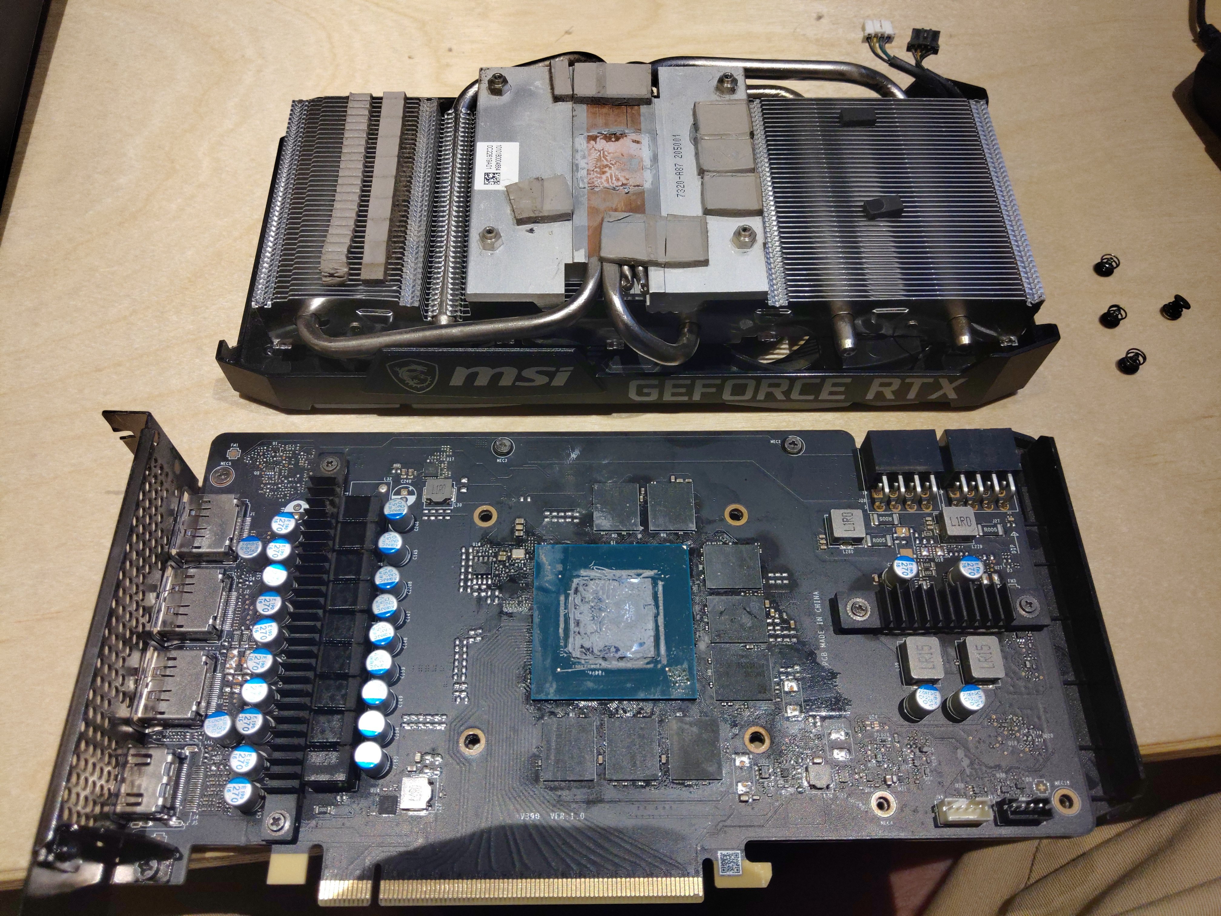
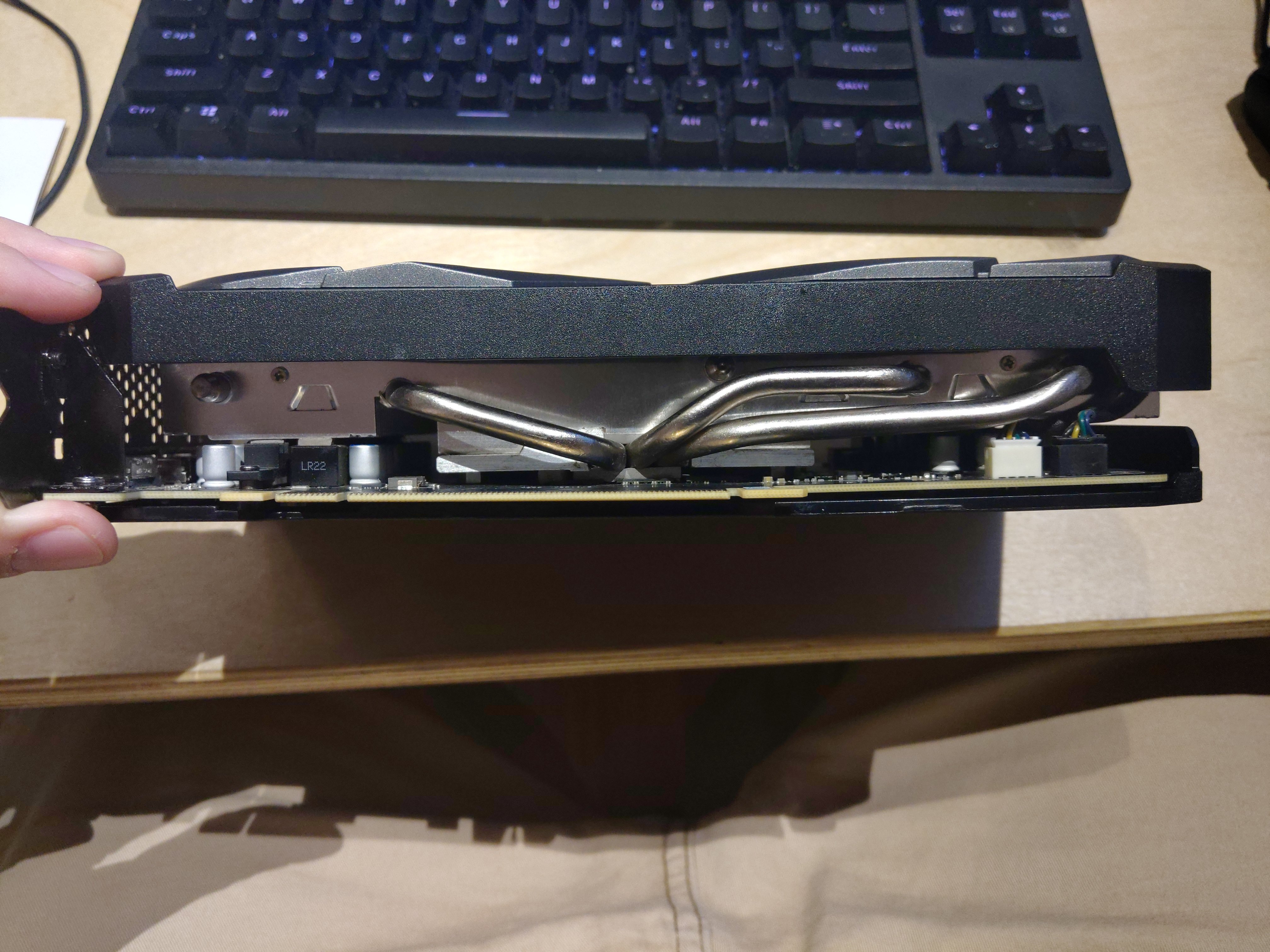
It is just basically a fiberglass panel. It has to get super hot for this to happen or the board is just made like junk. The only times I really see warping is when removing a bunch of stuff with a solder pot or heat gun, and I don't care about the board.
The GPU chip is super critical for full contact with the heatsink. The cooling mating surface of the package is the back side of the actual silicon die. It isn't in a carrier or thermal package that can average temperatures across the surface. The cooling element is basically sitting on the transistors of each circuit block. This means a lack of cooling over any specific circuit block can burn out the transistors in this region.
You're also likely getting bad performance with that much heat due to bleed over in adjacent nodes skewing results.
Your biggest secondary danger is with (technically any but mostly larger) multi layer ceramic capacitors. MLC's can short circuit due to flexing forces. The modern high capacity variety have extremely closely spaced plates inside that are only separated by a thin coating of ceramic. It only takes a microscopic fracture for these internal plates to offset and short circuit. This can be smaller than the unaided eye can see. It isn't hard to find them based on temperature and continuity.
In the end, it is just a fiberglass panel. There is nothing magic about it. If you have the fab skills, there is an easy/ugly solution to be had if you just get creative about it.

